Low Power DDR5 RAM for smartphones, tablets, and ultra-thin notebooks announced
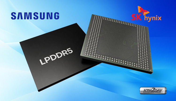

JEDEC Solid State Technology Association, the global leader in standards development for the microelectronics industry, announced the publication of JESD209-5, Low Power Double Data Rate 5 (LPDDR5). LPDDR5 will eventually operate at an I/O rate of 6400 MT/s, 50% higher than that of the first version of LPDDR4, which will significantly boost memory speed and efficiency for a variety of applications including mobile computing devices such as smartphones, tablets, and ultra-thin notebooks.
Samsung Electronics, the world leader in advanced memory technology, announced in June 2018 that it had successfully developed the industry’s first 10-nanometer (nm) class* 8-gigabit (Gb) LPDDR5 DRAM. Since bringing the first 8Gb LPDDR4 to mass production in 2014, Samsung has been setting the stage to transition to the LPDDR5 standard for use in upcoming 5G and Artificial Intelligence (AI)-powered mobile applications.
In addition, LPDDR5 offers new features designed for mission critical applications such as automotive.
LPDDR5 boasts a data rate of up to 6,400 megabits per second (Mb/s), which is 1.5 times as fast as the mobile DRAM chips used in current flagship mobile devices (LPDDR4X, 4266Mb/s). With the increased transfer rate, the new LPDDR5 can send 51.2 gigabytes (GB) of data, or approximately 14 full-HD video files (3.7GB each), in a second.
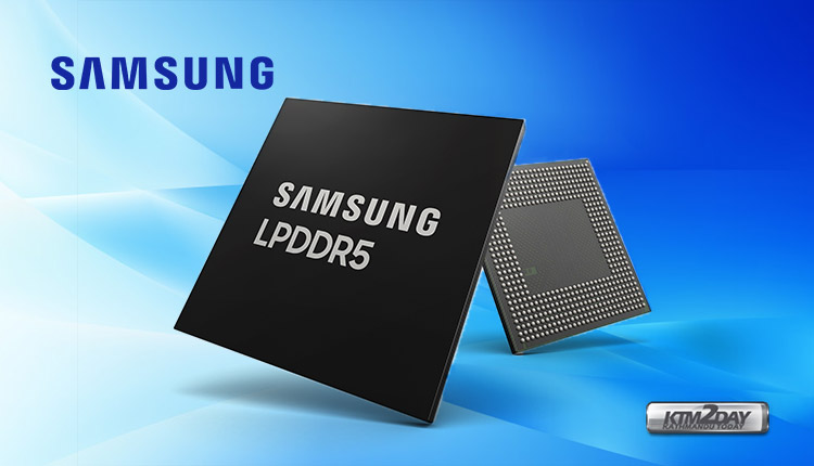
The previous gen LPDDR4 had a data rate of 3200 MT/s, LPDDR5 promises to have an enormous impact on the performance and capabilities of the next generation of portable electronic devices. To achieve this performance improvement, LPDDR5 architecture was redesigned; moving to 16Banks programmable architecture and multi-clocking architecture.
SK hynix claimed to be the first chipmaker to develop DDR5 DRAM chips that met JEDEC standards back in Nov 2018. The firm is said to be spending $107 billion building four memory chip factories. The fabrication facilities will be located on a 4.5 million square metre site south of Seoul, with work commencing from 2022.
LPDDR5 Key specification updates include:
- I/O throughput up to 6400 Mbps
- Signaling voltage – 250mV
- Non-Target ODT for DQ was added to support higher data rate
- Signal integrity enhancement by DFE
- Clocking architecture: WCK & Read Strobe (RDQS) added to support higher data rate
- Programmable Multi-bank organization (8Banks, 4Bank groups/4Banks, and 16Banks)
- Selectable background and command based ZQ calibration
- Low-power features added include
- Dynamic Frequency and Voltage Scaling for Core and I/O
- Selectable differential and single-ended CK, WCK, and RDQS
- Partial array self-refresh and auto-refresh
- Low power read/write operation with Data-Copy and Write-X functions
- Function/Features targeting automotive applications including
- Optional Link ECC
- New packaging definition
JEDEC is the global leader in the development of standards for the microelectronics industry. Thousands of volunteers representing nearly 300 member companies work together in over 100 JEDEC committees and task groups to meet the needs of every segment of the industry, manufacturers and consumers alike.


